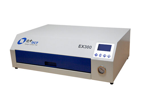
EL400 & EX300 UV Exposure Units – High‑Precision Imaging Transfer for PCB & Solder Mask

Product Description
The EX Series UV Exposure Units from DCT deliver advanced line‑scan exposure technology for precise imaging transfer in PCB fabrication and related processes. Covering models EL400 and EX300, the series provides a range of processing capabilities to accommodate dry‑film photoresist exposure for single‑sided and double‑sided PCBs, as well as solder mask imaging for nameplates and hollow‑out components.
The EL400 utilizes an imported UV‑LED light source with narrow spectral bandwidth and minimal stray radiation, resulting in low thermal impact and highly accurate exposure dimensions. Its PMMA light guide plate ensures high light transmittance and excellent uniformity, supporting 25μm line/space resolution for fine‑line circuit applications.
The EX300 is equipped with a UV‑A actinic fluorescent tube and double‑sided Mylar film vacuum frame, providing reliable double‑sided exposure. With a resolution of 75μm line/space and a capacity of 120 panels per hour, the EX300 is optimized for high‑throughput PCB prototyping and small‑batch production.
Both models feature vacuum holding (≤0.6 MPa) and ergonomic benchtop designs, making the EX Series ideal for R&D labs, universities, PCB prototyping centers, and small‑scale manufacturing facilities requiring UV exposure, dry‑film photoresist imaging, or solder mask transfer with reliable, repeatable quality.
Key Features
Shared Features (Both Models)
Advanced Line‑Scan Technology – Ensures parallel output light for consistent exposure across the entire working area.
Vacuum Holding System – ≤0.6 MPa vacuum secures substrates during exposure, preventing misalignment.
Benchtop Compact Design – Space‑saving footprint suitable for laboratory benches and small production lines.
User‑Friendly Operation – Straightforward controls for quick setup and reliable day‑to‑day performance.
Wide Application Range – Supports dry‑film photoresist exposure for PCBs, solder mask imaging for nameplates, and hollow‑out component processing.
Model‑Specific Features
| Feature | EL400 | EX300 |
|---|---|---|
| Exposure Technology | UV‑LED (进口 LED 紫外光源) – narrow spectrum, low stray radiation, minimal thermal effect | UV‑A fluorescent tube – proven actinic light source for reliable photoresist exposure |
| Resolution Capability | 25μm line/space – ideal for fine‑line, high‑density circuit designs | 75μm line/space – suitable for standard PCB prototyping |
| Light Uniformity | PMMA light guide plate – high transmittance and uniformity | Double‑sided Mylar film vacuum frame – ensures even UV distribution |
| Throughput | 30 panels/hour – optimized for precision over speed | 120 panels/hour – high‑capacity for production environments |
| Double‑Sided Exposure | Single‑side exposure (dual‑side capable with flip operation) | Integrated double‑sided exposure with Mylar film frame |
| Typical Application | High‑precision R&D, fine‑line circuits, solder mask imaging | High‑volume prototyping, double‑sided PCB production |
Technical Specifications
| Parameter | EL400 | EX300 |
|---|---|---|
| Min. Resolution Line Width | 25 μm | 75 μm |
| Min. Resolution Line Spacing | 25 μm | 75 μm |
| Max. Exposure Area | 400 mm × 300 mm | 305 mm × 230 mm |
| Capacity (Throughput) | 30 PNL/h | 120 PNL/h |
| Vacuum Requirement | ≤0.6 MPa | ≤0.6 MPa |
| Light Source | UV LED (395 nm) | UV‑A actinic fluorescent tube (365 nm) |
| Transparent Material | PMMA light guide plate | Mylar film (vacuum frame) |
| Exposure Type | Single‑side (double‑side capable with manual flip) | Double‑side integrated |
| Power Supply | 220 VAC / 50 Hz | 220 VAC / 50 Hz |
| Power Consumption | 0.3 kW | 0.25 kW |
| Equipment Weight | 25 kg | 20.5 kg |
High-Precision, High-Quality: Setting the New Standard in Compact Depaneling
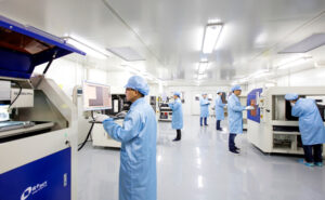
As electronics continue to evolve toward higher density, smaller form factors, and more irregular board geometries, conventional depaneling methods often fall short. DCT delivers an environmentally friendly, fast, precise, and reliab
le laser cutting solution—engineered to meet the demands of next-generation PCB assembly.
Stress‑Free Cutting
Even with components placed extremely close to the cut line, our laser process introduces zero mechanical stress, protecting sensitive parts and ensuring long‑term reliability.
Precise Thermal Management
We match laser type and processing parameters to the thermal characteristics of each board, significantly reducing heat‑affected zones and preventing damage to adjacent components.
Clean, Contaminant‑Free Operation
During cutting, gases and ablation byproducts are extracted in real time, minimizing contamination risk and maintaining a clean assembly environment.
Our Equipment
Equipping projects with powerful machines
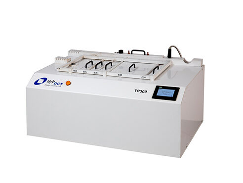
TP Series Through‑Hole Plating Equipment – Carbon Film Metallization for PCB Prototyping

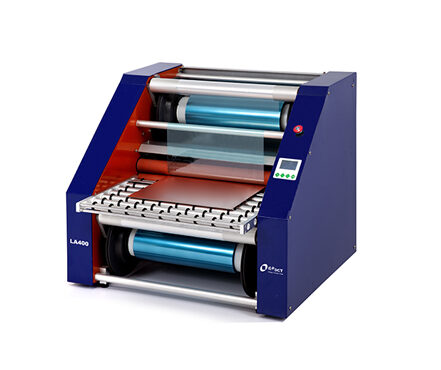
LA Series Dry Film Laminator – Precision Desktop Laminating for PCB & Substrate Manufacturing

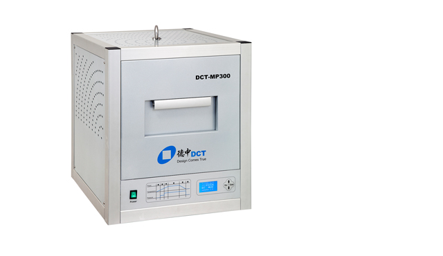
MP300 & MP300D Multilayer PCB Lamination Presses – Compact & High‑Capacity Solutions for PCB Prototyping